Through this practical work we will describe sequential and combinatorial blocks in the form behavioral. We will thus see the impact of this writing on the inference of the blocks from the RTL scheme. We will then obtain the technological diagram from the previous diagram. The performance of the implementation will then be analyzed. Finally, by the physical implementation of the circuit we will test our code. This will require the definition of constraints for the assignment of legs of the circuit.
Goal : displaying value on a seven-segments display

1. VHDL Implementation
We want to create the display block to view the modem configuration mode (mode input), using six seven-segment displays.
1.1 Circuit interface
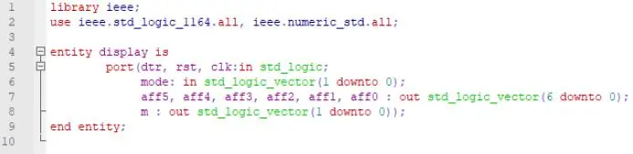
In a display.vhd file, we define the circuit interface using the following display entity:

We have the input and output signals of type std_logic and std_logic_vector.
1.2. BEH behavioral architecture
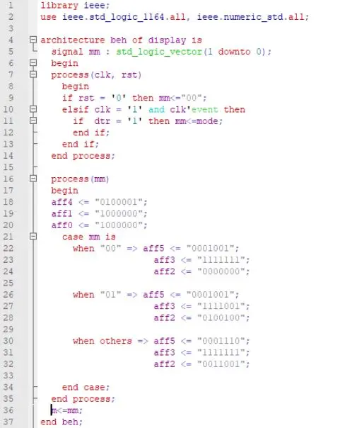
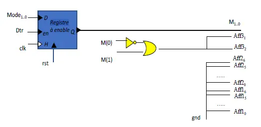
We define a BEH behavioral architecture based on the following ASM:

This definition is carried out with two processes. A synchronous process on clk and rst to describe the register transfer to be performed on mm or force to 00 on asynchronous rst true low. Another combinatorial process to describe the output combinations of the six displays as a function of mm by using a case statement.
We therefore used the internal signal mm because M is configured as an output only.
1.3 Testbench
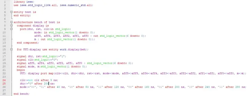
We have the following testbench:
1.4. BEH Simulation
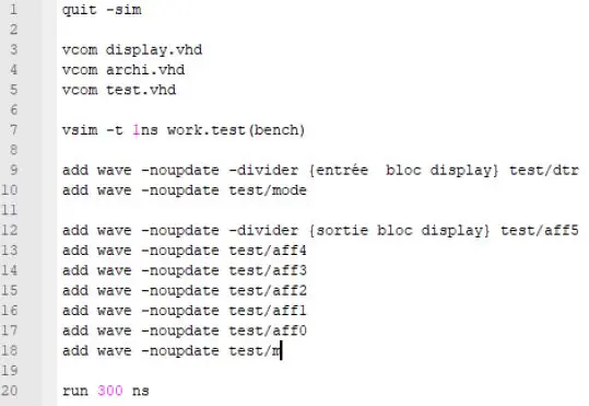
We write a display.tcl script for our BEH simulation of the block under Modelsim.
We obtain the following:
We obtain the following chronogram:

We have the expected behavior of ASM. When dtr is at ‘1’, synchronously M ← Mode and depending on its value, the displays show us the configuration mode of the modem, on aff0 and aff1 the transmission mode is indicated to us, bidirectional (FD) or alternate (HD), on the other four aff* the transmission rate in bps is indicated (400,800 or 1200). When dtr is ‘0’ the transfer does not apply.

We thus wish to physically test our behavioral architecture on the FPGA of the ALTERA card.
2. Synthesis of the VHDL description using interactive menus
2.1. Compilation
We launch precision synthesis RTL 17.1. The goal is to generate our architecture corresponding to the behavioral input description. The synthesis is carried out on the basis of generic gates.
We thus choose the CYCLONE II EP2C35F672C circuit at speed 6. After inserting our description and compilation we get the following implementation:
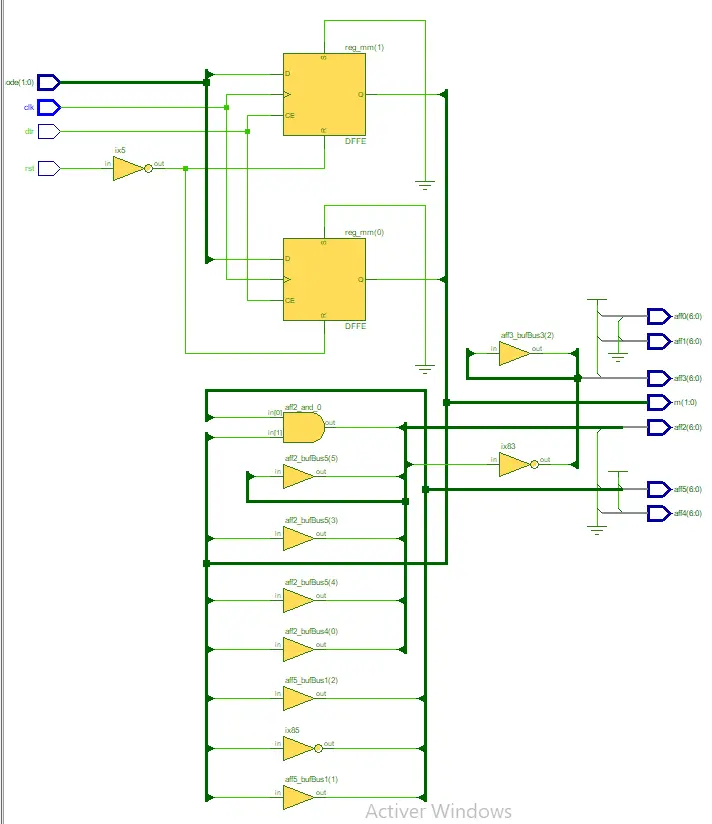
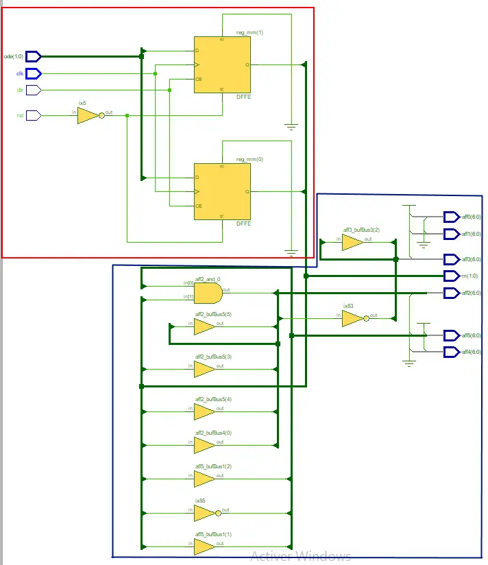
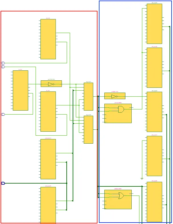
The sequential part in red is limited to the use of a synchronous register on each bit of M with a load control input connected to the dtr input.
The combinatorial part in blue is formed by logical operators to determine the values assigned to the segments as a function of M. We notice that some segments have a constant value, independent of M.
We therefore have an equivalence between our architecture and the expected one:
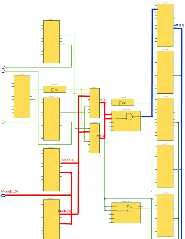
By requesting a backward to input trace on bit 2 of the display 3 we have the following diagram:
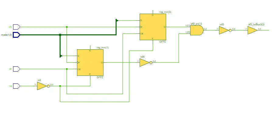
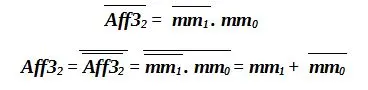
With the RTL scheme we get the following Boolean expression:

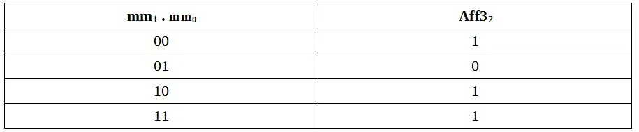
With our architecture we had the following truth table:
So we have :
2.3 Logical optimization
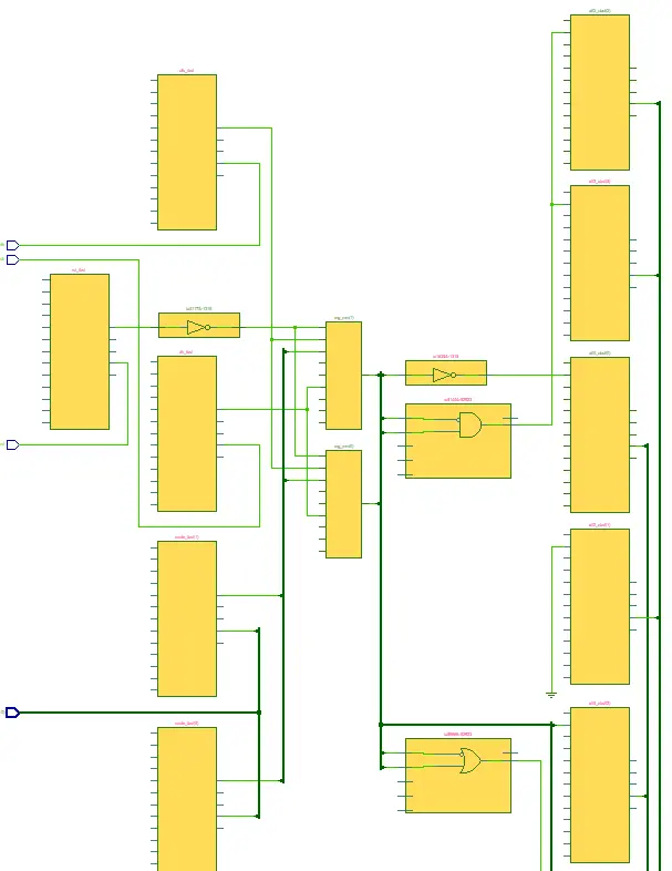
We are now asking for circuit optimization. The operation of the optimization tool is mainly based on the design constraints of the block. We set a clock constraint of 1 MHz, an output delay of 0.3 ns on the output m. Finally, we specify all other inputs and outputs as asynchronous.
We have the following technological diagram:
We carry out a report area on our optimization:
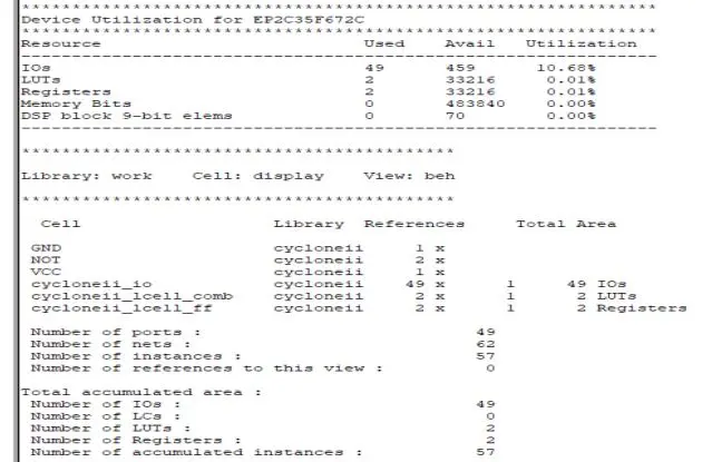
We can see on this report area that the optimization that is carried out is a surface optimization. We observe that on this report, the use of the processor is mainly due to the I / O and is 10.68%, the rest is weakly based on the 2 LUTs and the 2 registers.
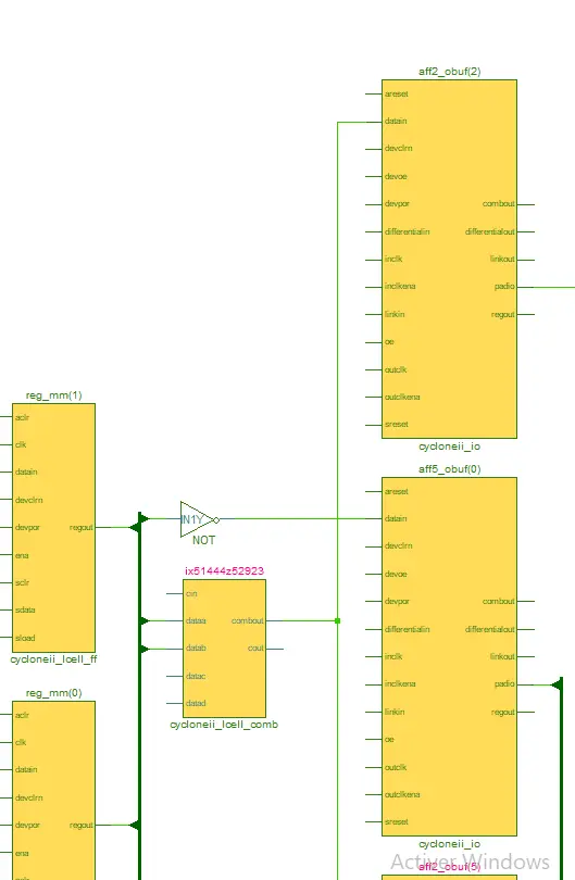
We visualize the critical path below, from the schematics panel:
The sequential part is in red, the combinatorial part is in blue.
We have the following diagram, leading from the Mode input, to bit 2 of display 3.
2.4. Routing placement
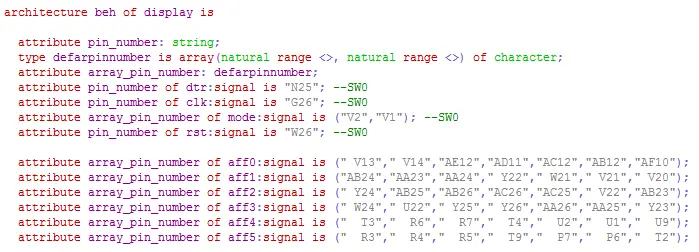
Physical testing of the circuit on the board's FPGA requires assigning the component legs to the model interface signals.
The following code is added in the declaration area of the BEH display architecture, so as to proceed with the assignment of the signals from the interface of the block to the legs of the FPGA, in accordance with the figure of the subject.
3. Synthesis from a command script
It is possible to run a script simulating the commands of the various tools of the synthesis flow. We define the synthesis script syntheseTP1.tcl below, taking up the different stages of the synthesis flow of the display block from the text commands.
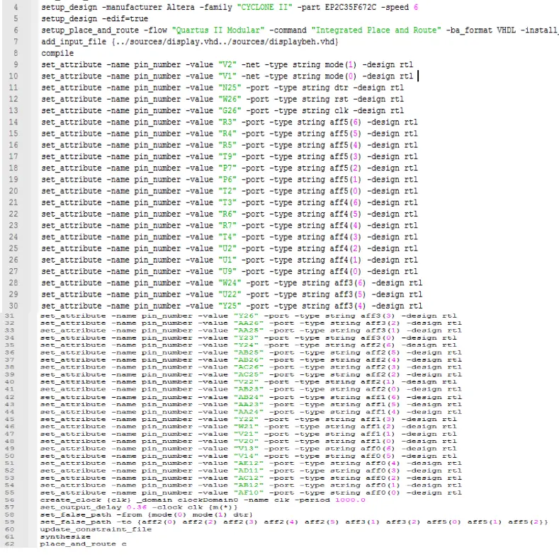
Through this script the legs are assigned to the different signals. For example, set_attribute –name pin_number –value Y23 -port -type string aff3 (3) -design rtl assigns pin Y23 to bit 3 of signal aff3.
4. FPGA circuit test
We now want to physically test our behavioral architecture on the FPGA of the Altera experiment board. The latter has the following characteristics:
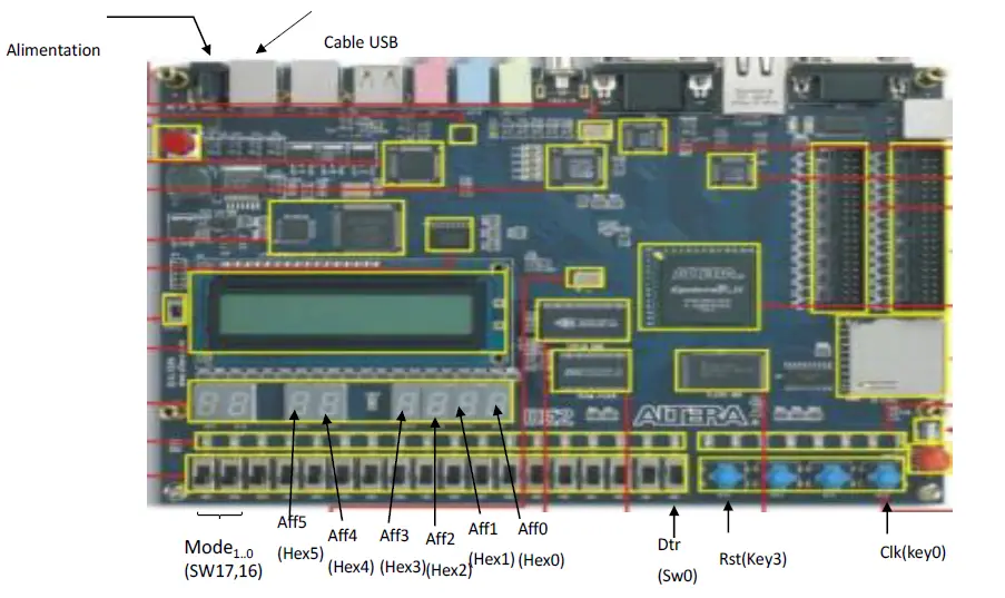
Mode = 00:
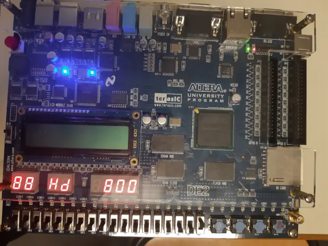
The transmission mode is alternate (HD), with a speed of 800 bps.
Mode = 01:

The transmission mode is alternate (HD), with a speed of 1200 bps.
Mode = 1X:
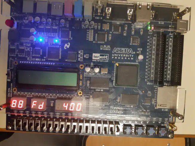
The transmission mode is bidirectional (FD), with a rate of 400 bps.
By setting dtr to ‘0’, the transfer is not made, which is quite consistent.
5. Conclusion
Through this practical work we have described sequential and combinatorial blocks in behavioral form. We also saw the impact of the VHDL writing on the inference of the blocks from the BEH schema. We also obtained the technological diagram from the previous diagram. The performance of the implementation was analyzed. Finally, through the physical implementation and pin assignment of the circuit, we were able to test our code to finally display value on a seven-segment display.